Introduction
Switch systems enable the routing of test equipment signals to multiple devices or test points, allowing for efficient measurement of multiple parameters. This is achieved through automatic sequential connection and disconnection of test equipment to the devices or test points.
Two specific use cases that are particularly relevant to me are PCB testing and measurement of analog sensors. While companies like Keithley offer specialized systems that would suffice for these tasks, I prefer a more hands-on approach so I decided to build my own system.
Features
I initially wanted to create a board that could be controlled directly from my Keithley 2450 digital I/O pins, but as I continued to work on the project, I added more and more features, resulting in a more flexible board that included:
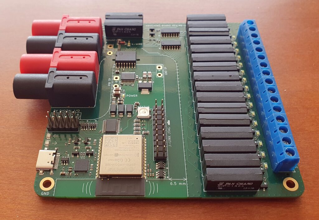
- Signal rating of 200 V (100 V switching) and 1A (500 mA switching).
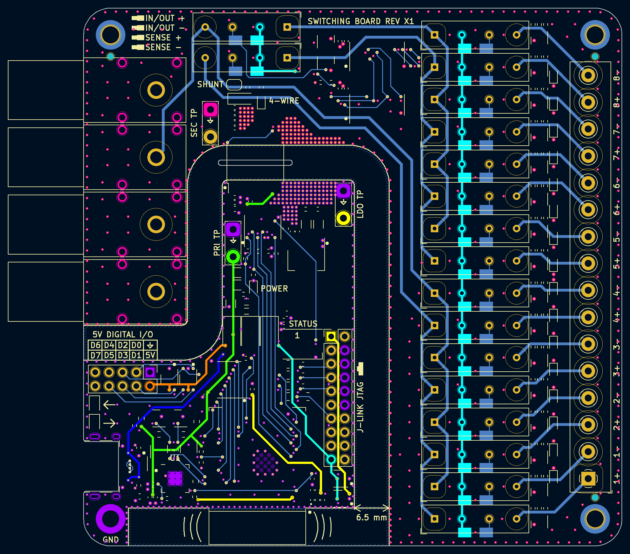
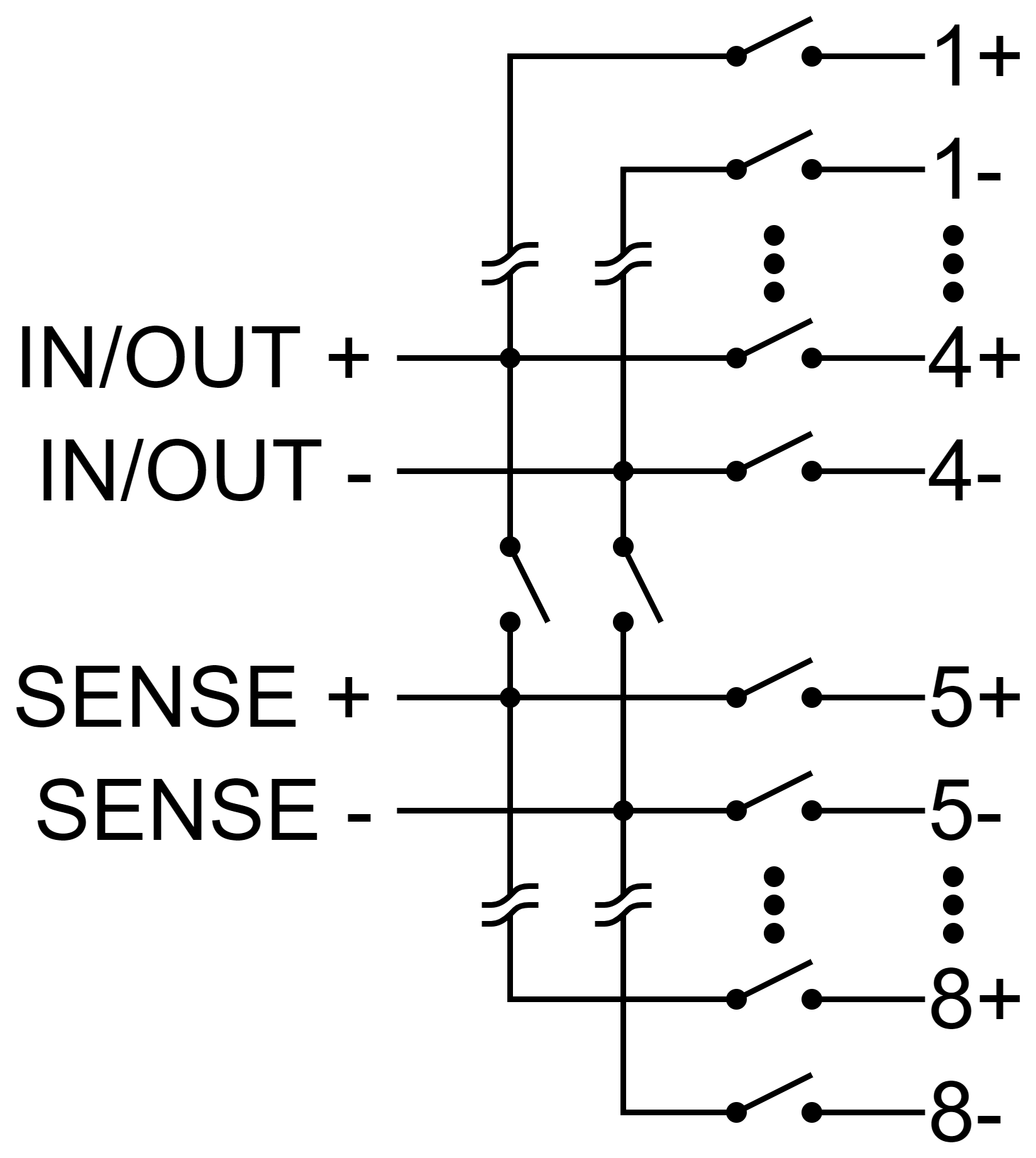
- 4 shrouded banana jacks input/output and sense connectors.
- 16 contact terminal block usable in single, 2- and 4-wire mode.
- Reed relays.
- Double isolation.
- 3 sources of power: USB, 5-V pins and J-Link JTAG connector
- USB, 5-V pins, and WIFI control.
- A J-Link JTAG connector.
- Power, TX, RX and relay status LEDs.
- An RGB programmable status LED.
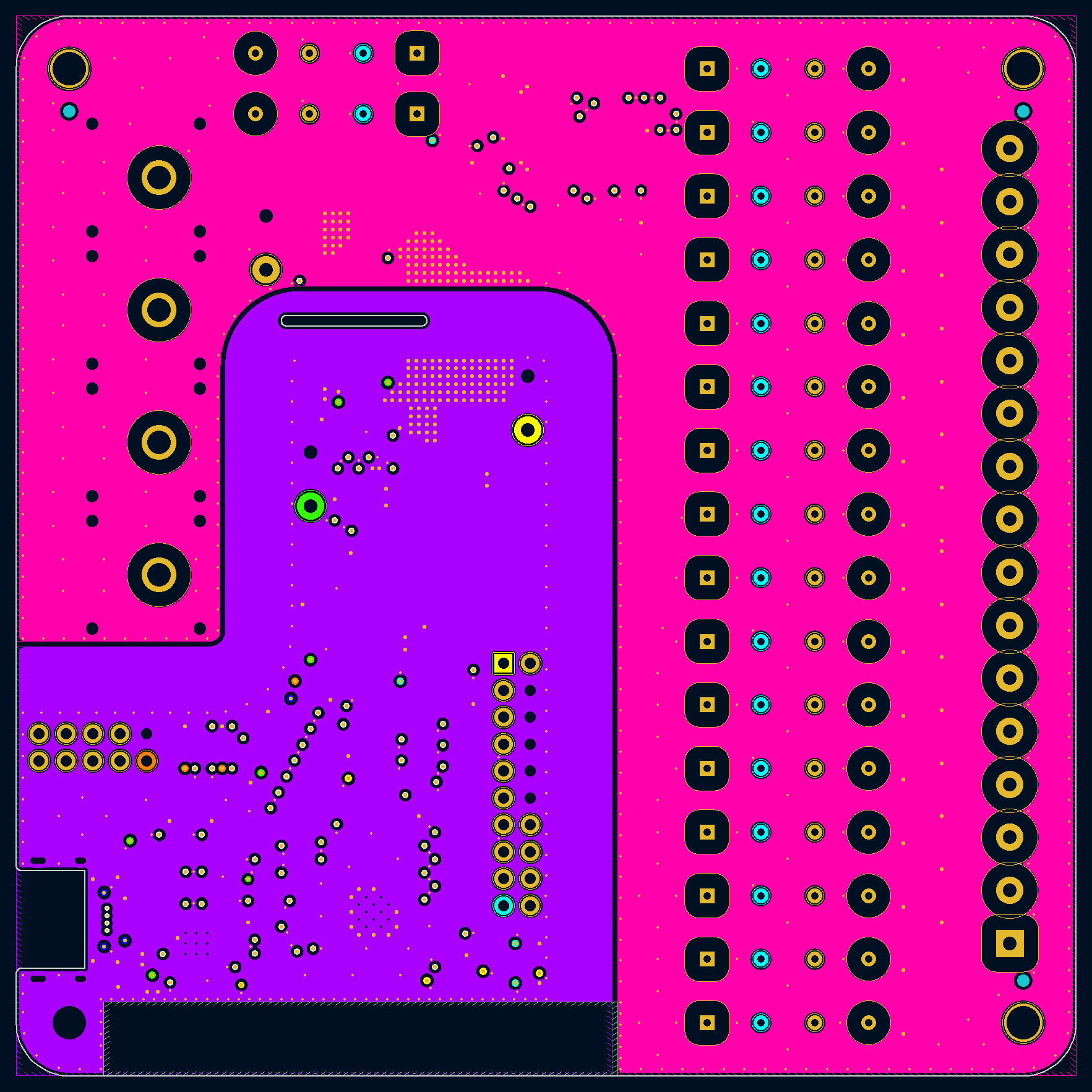
- 10 x 10 cm, 4 layer PCB with ground on both inner layers.
- ESP32 MCU.
- Silicon Labs CP2102 USB bridge.
Implementation Details
In the following paragraphs, I will attempt to provide an explanation for the reasoning behind some of the decisions made during the design phase.
Safety
If there is one area where one does not want to cut corners that area is safety. Since the board will be used with an SMU capable of delivering up to 200 V, and considering that it can operate connected through a USB to a PC, the last thing one wants is for the energy flow through an unexpected path and end up burning a computer, and SMU, or shocking the user. For the same reason may main concern during the design was to keep it contained within the tracks designed for that purpose. For this, I increased the track clearance to the maximum that I could within the constrained 100 x 100 mm PCB space, which ended up being 1.4 mm. To add an extra layer of safety I isolated the switching section from the low voltage section that contains the USB 3 connector, the 5 V pins, and the JTAG pins using an Analog ADuM6400. I used a clerance of 6.5 mm for the top and bottom layers and 0.5 mm for the internal layers. To reduce radiated noise I overlapped the inner ground planes so as to capacitively couple them.
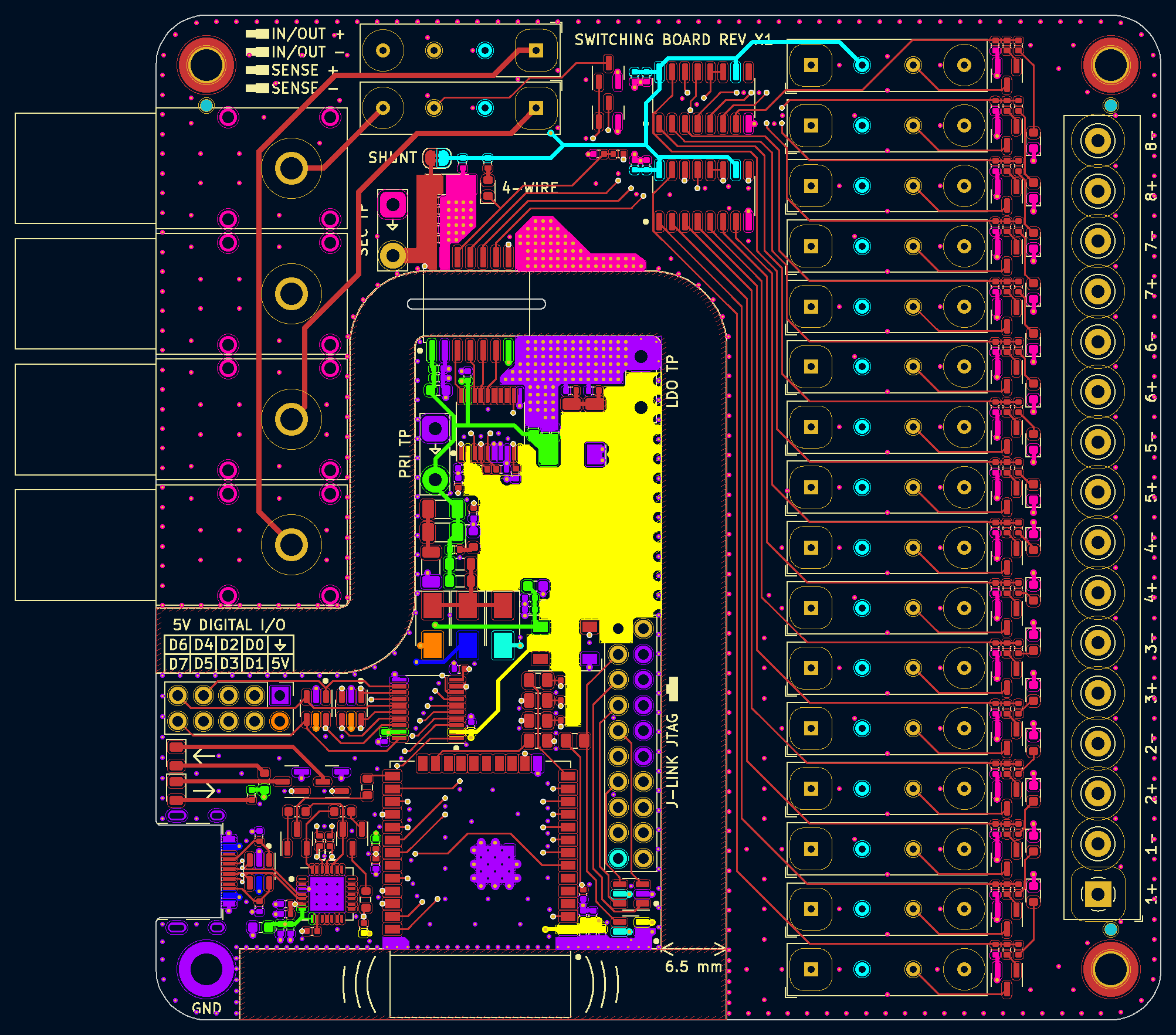

Switching topology
When selecting a relay, it is important to consider the trade-offs between different types. In my case, I opted for reed relays over electromagnetic relays due to their longer lifespan, despite the fact that electromagnetic relays typically handle higher currents. I also chose reed relays over solid state relays, as they have more suitable characteristics such no current leakage even though solid state relays may have a longer lifespan and handle higher currents.
To keep the relay count and PCB real-estate low I went for an 2- and 4-wire design. The network operates as either 8 2-wire channels or as 4 4-wire channels, but by manually connecting the positive and negative input channels it is possible operate it as 16 single wire channels.
Power
Power can be provided from three different 5 V power sources: the USB connector, the J-Link connector and the digital I/O connector. In the non-isolated section of the PCB, two rails are employed: one that is powered by the 5 V source and another that provides 3.3 V via an LDO. In contrast, the isolated section operates solely on a single 5 V rail, which is powered by the Analog ADuM6400.
Fabrication
The board was manufactured and assembled by JLPCB. In order to minimize expenses, the connectors (including banana, screw, USB, and 2.54 mm), the reed relays, the RGB LED, and the back side diodes were purchased from AliExpress and soldered manually at home.
Luckily I committed only two mistakes in the design. The first was a pull-up resistor that led to misconfiguration of the microcontroller module. The second was mistakenly setting the UART LEDs to turn off during transmission instead of the opposite way. The former mistake was rectified easily by removing the resistor, whereas for the latter, I opted not to correct it, as it did not affect the board’s functionality.