Introduction
Field-Programmable Gate Arrays (FPGAs) are fascinating integrated circuits (ICs) that just like central processing units (CPUs) can compute, but unlike them, operate in a completely different way. While a CPU implements an algorithm as a sequence of machine instructions, an FPGA implements it as interconnection and configuration of logic elements. Said differently, FPGA programming is closer to designing circuits than to writing instructions that get executed sequentially (unless the FPGA is programmed to operate as a processor, or it actually implements one).
FPGAs are usually programmed using hardware description languages (HDLs). These languages describe the digital logic so that the synthesis tool can generate the design implementation. There are two major HDLs: VHDL and Verilog. They are more or less equivalent, but some relevant differences are that Verilog is less verbose and uses a C-like syntax.
In this post I will give a practical introduction to how to program the Digilent Cmod S7 in Verilog.
Digilent Cmod S7
The Cmod S7 is an inexpensive board based on Xilinx’s 7th generation FPGAs. In contrast to previous FPGA generations, the 7th generation supports Vivado, Xilinx’s latest design tool.
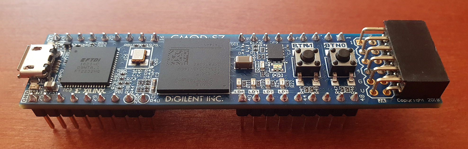
The board’s FPGA chip is connected to 4 green LEDs, 1 RGB LED, 2 push buttons, SPI Flash memory, an FTDI FT2232H USB-UART bridge, a 12 MHz crystal oscillator and an LTC3569 triple output buck regulator.
The FPGA designs that wrote use buttons and LEDs, so before starting, let’s see how they are wired to the FPGA.

The diagram shows that:
- The push buttons turn 1 (high) when pressed.
- The color components of the RGB LED are turned on by driving the signals to 0 (low).
- The 4 green LEDs are turned on by driving the signals to 1 (high).
Hello FPGA
The simplest design that can be programmed on an FPGA is one that drives an FPGA pin to either high or low. So to make things more interesting, I wrote a design that wires the LEDs to the push buttons.
To program in Verilog at least 2 files are required, a constraints (.xdc) file to set up the FPGA pins, and a Verilog (.v) file to specify the logic design.
Vivado’s constraints files contain Tcl commands that define the requirements that must be met for a design to be functional. Companies like Digilent provide constraints templates that need minor editing to use, but to make the post more informative I wrote my own minimal constraints file.
set_property -dict {PACKAGE_PIN D2 IOSTANDARD LVCMOS33} [get_ports {button[0]}];
set_property -dict {PACKAGE_PIN D1 IOSTANDARD LVCMOS33} [get_ports {button[1]}];

set_property -dict {PACKAGE_PIN F2 IOSTANDARD LVCMOS33} [get_ports {rgb[0]}];
set_property -dict {PACKAGE_PIN D3 IOSTANDARD LVCMOS33} [get_ports {rgb[1]}];
set_property -dict {PACKAGE_PIN F1 IOSTANDARD LVCMOS33} [get_ports {rgb[2]}];

set_property -dict {PACKAGE_PIN E2 IOSTANDARD LVCMOS33} [get_ports {led[0]}];
set_property -dict {PACKAGE_PIN K1 IOSTANDARD LVCMOS33} [get_ports {led[1]}];
set_property -dict {PACKAGE_PIN J1 IOSTANDARD LVCMOS33} [get_ports {led[2]}];
set_property -dict {PACKAGE_PIN E1 IOSTANDARD LVCMOS33} [get_ports {led[3]}];
The constraints file associated the specified pins to 3 busses:
- button: A 2 bit bus wired to each button.
- rgb: A 3 bit bus wired to each component of the RGB LED.
- led: A 4 bit bus wired to the 4 green LEDs.
module Top(button, rgb, led);
input wire [1 : 0] button;
output wire [2 : 0] rgb;
output wire [3 : 0] led;
assign rgb[0] = ~button[0];
assign rgb[1] = ~button[1];
assign rgb[2] = 1;
assign led[0] = button[0];
assign led[1] = button[1];
assign led[2] = button[0] | button[1];
assign led[3] = 1;
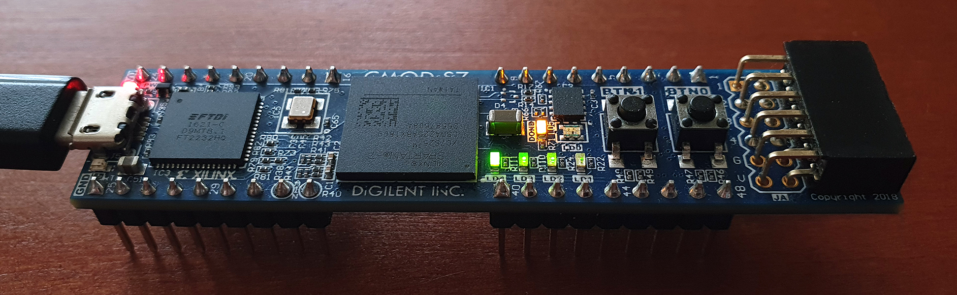
endmoduleAn this short video shows what the design does.
So how does the design work?
Modules are structures that encapsulate the design logic. The top module (Top) is the main module and encapsulates the logic of the complete design. The Top module is wired to the 3 busses, button (an input bus), rgb (an output bus) and led (an output bus).
The assign statement is used to connect the LEDs in the following way:
- Red component turns on (low) when pressing button 0. (“~” is the not logical operator)
- Green component turns on (low) when pressing button 1.
- Blue component stays off (high).
- LED 0 turns on (high) when pressing button 0.
- LED 1 turns on (high) when pressing button 1.
- LED 2 turns on (high) when pressing either button 0 or button 1 (“|” is the logical or operator).
- LED 3 stays on (high).

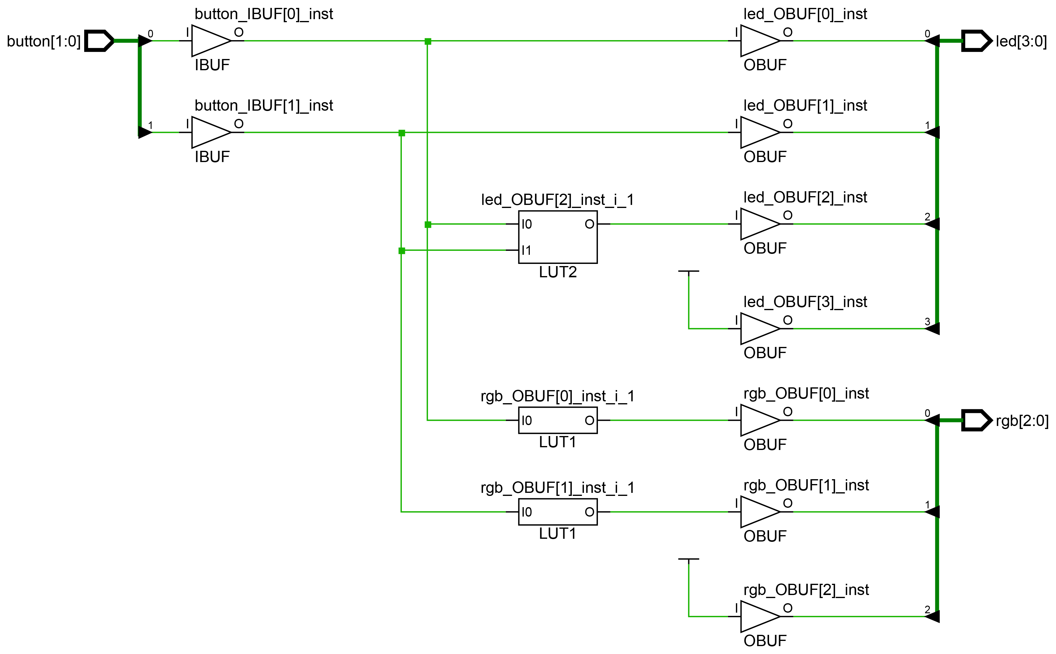
RTL schematics are almost as easy to understand as Verilog code. In contrast, the technology schematics tend to be orders of magnitude more complex and difficult to understand (even though this particular schematic is still very simple).
The technology schematic shows that the FPGA performs logic operations using look-up tables (LUTs). The way they work is by outputting the bit stored at the input index. The LUTs bit content is initialized so that their output is equivalent to the “emulated” logic operations (e.g., the not operator is implemented with the LUT1 primitive by setting the index 0 to 1, and the index 1 to 0).
IBUF and OBUF are input and output buffers and basically set the pins as either input or output.
The process of converting an abstract representation of a design into technology-specific logic primitives is called inference. Through inference code can be made portable across multiple FPGA platforms and can be optimized as needed for performance, area or power. The software analogy to inferring would be compiling.
In contrast, instantiation is the process where the primitives are specified in the code. This gives the highest control of the design, but at the cost of loss of portability and higher complexity. The software analogy to instantiating would be assembling.
There is no need to stick to a single approach, both approaches can be used together.
Let’s see how the previous design can be written by manually setting the LUTs to act as logic operators.
module Top(button, rgb, led);
    input  wire [1 : 0] button;
    output wire [2 : 0] rgb;
    output wire [3 : 0] led;

    LUT1 #(.INIT(2'b01)) rgb0 (.O(rgb[0]), .I0(button[0]));
    LUT1 #(.INIT(2'b01)) rgb1 (.O(rgb[1]), .I0(button[1]));
    assign rgb[2] = 1;

    assign led[0] = button[0];
    assign led[1] = button[1];
    LUT2 #(.INIT(4'b1110)) led2 (.O(led[2]), .I0(button[0]), .I1(button[1]));
    assign led[3]   = 1;
endmodule
The instanced code is identical to the inferred code, except for the lines 6, 7 and 12, where LUTs are instantiated to perform logical operations. To instantiate a LUT the table must be initialized (.INIT) and the input (I0, I1) and output (.O) must be wired.
A not requires the LUT to have a 1 at the index 0, and 0 at index 1, this is done initializing LUT1 to the binary “01” (2’b01). Analogously an or operator requires a LUT2 (2 inputs) initialized to the binary “1110” (4’b1110).
The buffering primitives can also be manually instantiated, but to keep things simple I let the synthesis tool infer them.
A complete list of all the available primitives can be found in a 600 pages document called: Vivado Design Suite 7 Series FPGA and Zynq-7000 SoC Libraries Guide (Code ug953).
PWM-regulated LED Brightness
Combinational logic circuits are characterized by output signals that depend only on the actual input signal values. With combinational logic it is not possible to generate an output that depends on past signals or states. Sequential logic solves this, but requires a clock signal.
The Cmod S7 includes a 12 MHz crystal oscillator connected to pin M9. However, it is possible to divide or multiply the clock frequency using the mixed-mode clock manager (MMCM) primitive if a design requires a different frequency.
To show how sequential logic works I wrote a simple design that uses the FPGA clock to output a pulse width modulation (PWM) signals to the board LEDs.
set_property -dict {PACKAGE_PIN M9 IOSTANDARD LVCMOS33} [get_ports {clk}];

set_property -dict {PACKAGE_PIN F2 IOSTANDARD LVCMOS33} [get_ports {rgb[0]}];
set_property -dict {PACKAGE_PIN D3 IOSTANDARD LVCMOS33} [get_ports {rgb[1]}];
set_property -dict {PACKAGE_PIN F1 IOSTANDARD LVCMOS33} [get_ports {rgb[2]}];

set_property -dict {PACKAGE_PIN E2 IOSTANDARD LVCMOS33} [get_ports {led[0]}];
set_property -dict {PACKAGE_PIN K1 IOSTANDARD LVCMOS33} [get_ports {led[1]}];
set_property -dict {PACKAGE_PIN J1 IOSTANDARD LVCMOS33} [get_ports {led[2]}];
set_property -dict {PACKAGE_PIN E1 IOSTANDARD LVCMOS33} [get_ports {led[3]}];
module Top(clk, rgb, led);
input wire clk;
output wire [2 : 0] rgb;
output wire [3 : 0] led;
assign rgb = 3'b111;
Pwm pwm0 (clk, 1, led[0]);
Pwm pwm1 (clk, 4, led[1]);
Pwm pwm2 (clk, 16, led[2]);
Pwm pwm3 (clk, 64, led[3]);
endmodule
module Pwm(clk, value, state);
input wire clk;
input wire [6 : 0] value;
output reg state;
reg [5 : 0] counter = 0;
always @(posedge clk)
begin
counter = counter + 1;
state = (counter < value);
end
endmodule
The constraints file sets the clock wire (clk), and the LED busses (rgb and led) up. The clock signal can be used like any other signal, but what makes it special is that it switches from 0 to 1 and back at a defined frequency.
The Verilog design defines 2 modules, a top module (Top) and a PWM module (Pwm). The top module turns off the RGB LED, and instantiates the PWM module 4 times. Each PWM instance generates a different output signal to each of the 4 green LEDs.
The PWM module takes 3 parameter, a clock signal input (clk), a duty cycle input (value) and a PWM output (state). The value parameter specifies how many time units state stays high during each PWM cycle (arbitrarily set to 64 time units).
The module uses a 6 bit counter reg (counter) to count the passed time since the beginning of the PWM cycle. In contrast to wire, reg does not need to be continuously driven, and can retain values.
The always block describes things that will repeat indefinitely at every clk rising edge (posedge clk). Clock rising edges increase the counter by one until it wraps around. state on the other side is set to 1 if counter < value, or 0 otherwise.
The design sets the PWM frequency to 187.5 kHz (12 MHz / 64), and the duty cycle of LED 0 to 1/64, LED 1 to 4/64, LED 2 to 16/64 and LED 3 to 64/64.
As designs get more complex, debugging becomes more important. There many alternatives to debug FPGAs, but one of the simplest is to write a testbench to simulate the circuit behavior.
Testbenches are programs that are used to test designs and verify their correctness. As they run in a simulator (not in the FPGA), they can use non-synthesizable features like for-loops, printing to the screen and reading and saving files.
To verify the correctness of the complete design I wrote a minimal testbench that instantiates Top.
module TopTb();
    reg  clk = 0;
    wire [2 : 0] rgb;
    wire [3 : 0] led;

    Top top (clk, rgb, led);

    always
        #1 clk = ~clk;
endmodule
The testbench controls the clock signal (clk) and switches its state every single time unit. This is done with #1, which tells the simulator to wait 1 time unit before continuing (delays are not synthesizable an can only be used in testbenches).
The testbench generated the following signals.
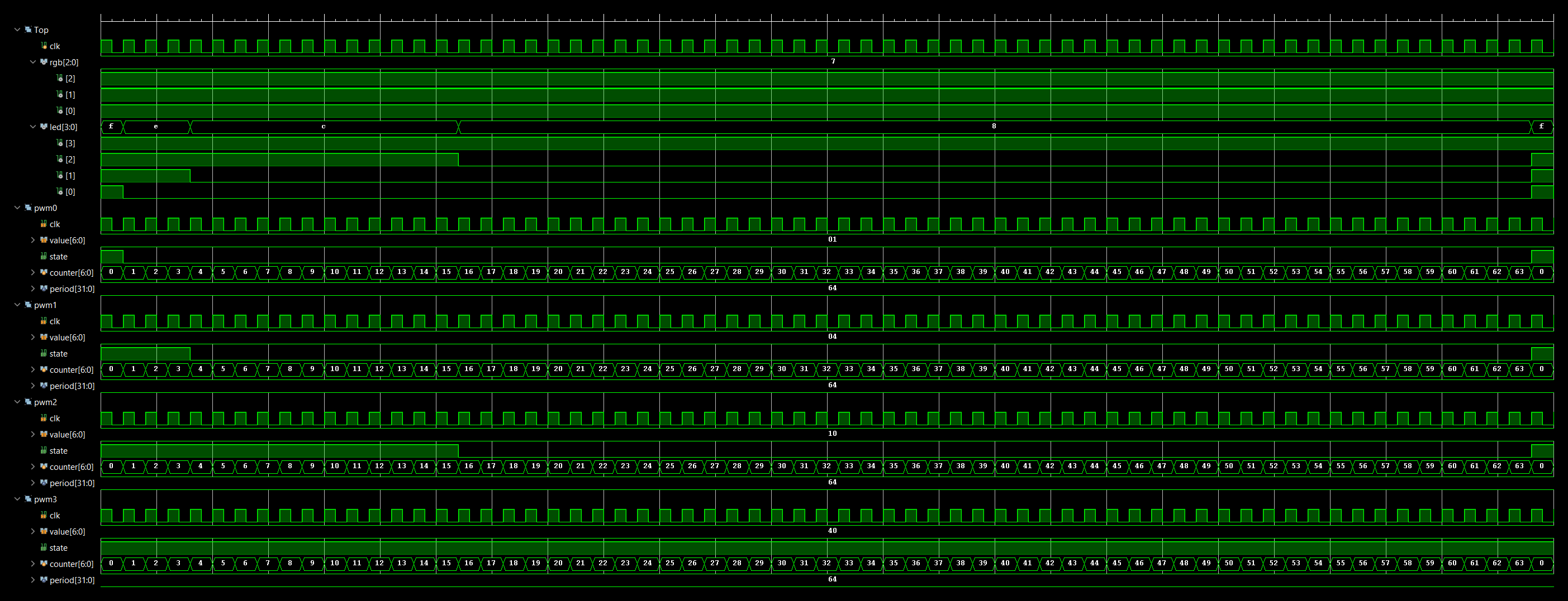
The generated traces show that the PWM period is 64 time units, and that the PWM signal goes high when counter = 0, and goes low when counter = value.
These results validate that the design is correct.
Conclusion
Learning to program FPGAs can be very time consuming. First, the tools are complex and non-standard. Second, the programming paradigm is different, it is more about pipelining operations than sequencing instructions as in traditional programming. Third, debugging is also completely different than in traditional programming, as it is not possible to directly detect what part of the code originates the bug. And fourth, the code can be hard to maintain and make it portable across platforms.
As a beginner one the most difficult parts is to learn how to translate an algorithm into an FPGA design. In this post I covered the very basics of FPGA HDL programming, mostly to give the intuition on how FPGAs operate and how they are programmed. Complex HDL designs still rely on the same building blocks (i.e. combinational and sequential logic), so even though the shown designs are simple, they illustrate well how FPGAs are programmed.
The code is available on GitHub.